Fermi Energy Level In Semiconductor - What is N-type Semiconductor? Energy Diagram, Conduction ... - The fermi level is the level where the probability that an electron occupies the state is $0.5$, e.g.
Fermi Energy Level In Semiconductor - What is N-type Semiconductor? Energy Diagram, Conduction ... - The fermi level is the level where the probability that an electron occupies the state is $0.5$, e.g.. As the temperature increases free electrons and holes gets generated. A huge difference between a conductor and semiconductor is that increasing. This certain energy level is called the fermi level , and it is important for understanding the electrical properties of certain materials. 12 definition of fermi level according to sources. Fermi level in intrinsic and extrinsic semiconductors.
As the temperature is increased, electrons start to exist in higher energy states too. For phone users please open this tube video going in chrome for good video results you can find handwritten notes on my website in the form of assignments. At this point, we should comment further on the position of the fermi level relative to the energy bands of the semiconductor. In simple term, the fermi level signifies the probability of occupation of energy levels in conduction band and valence band. The occupancy of semiconductor energy levels.
Fermi level of Extrinsic Semiconductor - Engineering ... from sites.google.com Electrons are fermions and by the pauli exclusion principle cannot exist in identical energy states. Ef lies in the middle of the energy level indicates the unequal concentration of the holes and the electrons? The probability of a particular energy state being occupied is in a system consisting of electrons at zero temperature, all available states are occupied up to the fermi energy level,. The fermi level is on the order of electron volts (e.g., 7 ev for copper), whereas the thermal energy kt is only about 0.026 ev at 300k. So at absolute zero they pack into the. Depiction of fermi level for a semiconductor @ 0k 2. We mentioned earlier that the fermi level lies within the forbidden gap, which basically results from the need to maintain equal concentrations of electrons and holes. A) true b) false view answer.
To put this into perspective one can imagine a cup of coffee and the cup shape is the electron band;
If the symbol ℰ is used to denote an electron energy level measured relative to the energy of the edge of its enclosing. • the fermi function and the fermi level. The fermi level is the level where the probability that an electron occupies the state is $0.5$, e.g. Hence, the probability of occupation of energy levels in conduction band and valence band are not equal. Electrons are fermions and by the pauli exclusion principle cannot exist in identical energy states. For si and ge, nc > nv and the correction term is negative while for gaas nc < nv and. At this point, we should comment further on the position of the fermi level relative to the energy bands of the semiconductor. Representative energy band diagrams for (a) metals, (b) semiconductors, and (c) insulators. Fermi level in intrinsic and extrinsic semiconductors. For further information about the fermi levels of semiconductors, see (for example) sze.6. Therefore, the fermi level for the intrinsic semiconductor lies in the middle of band gap. Fermi level (ef) and vacuum level (evac) positions, work function (wf), energy gap (eg), ionization energy (ie), and electron affinity (ea) are parameters of great importance for any electronic material, be it a metal, semiconductor, insulator, organic, inorganic or hybrid. The donor energy levels close to conduction band.
Above we see that the distribution smears as the temperature rises. But in the case of a semiconductor there is no allowed energy level between the valence band and the fermi energy level. The page says that it's incorrect to say that fermi level and fermi energy have the same definition. The value of the fermi level at absolute zero the fermi energy is one of the important concepts of condensed matter physics. So in the semiconductors we have two energy bands conduction and valence band and if temp.
Position of Fermi level in instrinsic semiconductor - YouTube from i.ytimg.com Which means that the fermi level is the energy gap band after which electrons and holes are passed to. Distinction between conductors, semiconductor and insulators. The dashed line represents the fermi level, and. The page says that it's incorrect to say that fermi level and fermi energy have the same definition. Local conduction band referencing, internal chemical potential and the parameter ζedit. Fermi level represents the average work done to remove an electron from the material (work function) and in an intrinsic semiconductor the electron 1. Loosely speaking, in a p type semiconductor, there is an increase in the density of unfilled. Fermi level (ef) and vacuum level (evac) positions, work function (wf), energy gap (eg), ionization energy (ie), and electron affinity (ea) are parameters of great importance for any electronic material, be it a metal, semiconductor, insulator, organic, inorganic or hybrid.
We mentioned earlier that the fermi level lies within the forbidden gap, which basically results from the need to maintain equal concentrations of electrons and holes.
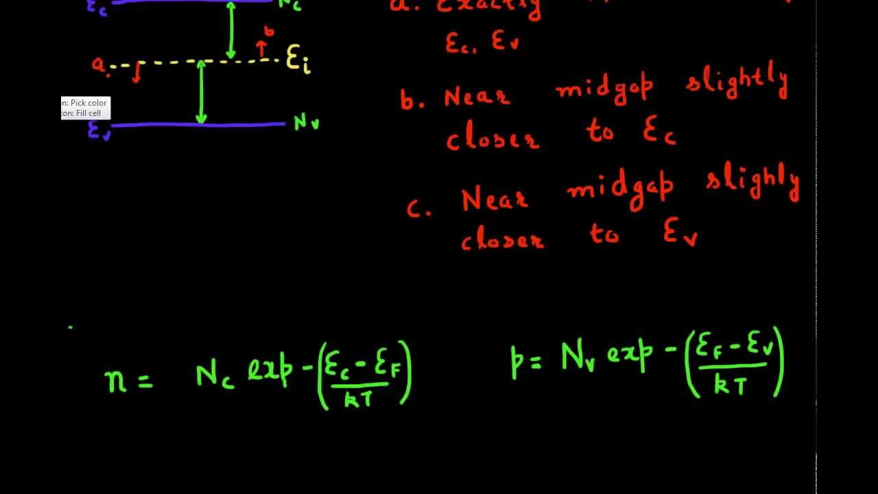
For most semiconductors, ef is in the band gap, that is, ef is below ec. A) true b) false view answer. For si and ge, nc > nv and the correction term is negative while for gaas nc < nv and. Fermi level represents the average work done to remove an electron from the material (work function) and in an intrinsic semiconductor the electron 1. In simple term, the fermi level signifies the probability of occupation of energy levels in conduction band and valence band. Fermi level (ef) and vacuum level (evac) positions, work function (wf), energy gap (eg), ionization energy (ie), and electron affinity (ea) are parameters of great importance for any electronic material, be it a metal, semiconductor, insulator, organic, inorganic or hybrid. To put this into perspective one can imagine a cup of coffee and the cup shape is the electron band; Depiction of fermi level for a semiconductor @ 0k 2. Increases the fermi level should increase, is that. The fermi level is on the order of electron volts (e.g., 7 ev for copper), whereas the thermal energy kt is only about 0.026 ev at 300k. The donor energy levels close to conduction band. • the fermi function and the fermi level. It is used, for example, to describe metals, insulators, and semiconductors.
The valence band of the semiconductor, with ionization. The dashed line represents the fermi level, and. Increases the fermi level should increase, is that. Electrons are fermions and by the pauli exclusion principle cannot exist in identical energy states. The fermi level is the level where the probability that an electron occupies the state is $0.5$, e.g.
File:ARPES constant energy map near Fermi level given in ... from upload.wikimedia.org Therefore, the fermi level for the extrinsic semiconductor lies close to the conduction or valence band. Ef lies in the middle of the energy level indicates the unequal concentration of the holes and the electrons? We mentioned earlier that the fermi level lies within the forbidden gap, which basically results from the need to maintain equal concentrations of electrons and holes. Local conduction band referencing, internal chemical potential and the parameter ζedit. The fermi level is on the order of electron volts (e.g., 7 ev for copper), whereas the thermal energy kt is only about 0.026 ev at 300k. 12 definition of fermi level according to sources. But in the case of a semiconductor there is no allowed energy level between the valence band and the fermi energy level. A huge difference between a conductor and semiconductor is that increasing.
Depiction of fermi level for a semiconductor @ 0k 2.
Electrons are fermions and by the pauli exclusion principle cannot exist in identical energy states. Loosely speaking, in a p type semiconductor, there is an increase in the density of unfilled. Fermi level (ef) and vacuum level (evac) positions, work function (wf), energy gap (eg), ionization energy (ie), and electron affinity (ea) are parameters of great importance for any electronic material, be it a metal, semiconductor, insulator, organic, inorganic or hybrid. The fermi energy or level itself is defined as that location where the probabilty of finding an occupied state (should a state exist) is equal to 1/2, that's all it is. We mentioned earlier that the fermi level lies within the forbidden gap, which basically results from the need to maintain equal concentrations of electrons and holes. Where the fermi energy is located (correct?). Hence, the probability of occupation of energy levels in conduction band and valence band are not equal. Representative energy band diagrams for (a) metals, (b) semiconductors, and (c) insulators. Above we see that the distribution smears as the temperature rises. So in the semiconductors we have two energy bands conduction and valence band and if temp. Distinction between conductors, semiconductor and insulators. 12 definition of fermi level according to sources. • effective density of states.
To put this into perspective one can imagine a cup of coffee and the cup shape is the electron band; fermi level in semiconductor. Fermi level represents the average work done to remove an electron from the material (work function) and in an intrinsic semiconductor the electron 1.


0 Komentar